Original Link: https://www.anandtech.com/show/7003/the-haswell-review-intel-core-i74770k-i54560k-tested
The Haswell Review: Intel Core i7-4770K & i5-4670K Tested
by Anand Lal Shimpi on June 1, 2013 10:00 AM EST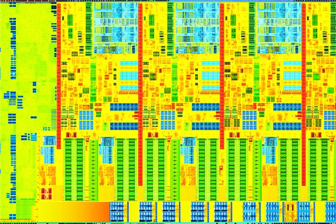
This is a very volatile time for Intel. In an ARM-less vacuum, Intel’s Haswell architecture would likely be the most amazing thing to happen to the tech industry in years. In mobile Haswell is slated to bring about the single largest improvement in battery life in Intel history. In graphics, Haswell completely redefines the expectations for processor graphics. There are even some versions that come with an on-package 128MB L4 cache. And on the desktop, Haswell is the epitome of polish and evolution of the Core microprocessor architecture. Everything is better, faster and more efficient.
There’s very little to complain about with Haswell. Sure, the days of insane overclocks without touching voltage knobs are long gone. With any mobile-first, power optimized architecture, any excess frequency at default voltages is viewed as wasted power. So Haswell won’t overclock any better than Ivy Bridge, at least without exotic cooling.
You could also complain that, for a tock, the CPU performance gains aren’t large enough. Intel promised 5 - 15% gains over Ivy Bridge at the same frequencies, and most of my tests agree with that. It’s still forward progress, without substantial increases in power consumption, but it’s not revolutionary. We compare the rest of the industry to Intel’s excellent single threaded performance and generally come away disappointed. The downside to being on the top is that virtually all improvements appear incremental.
The fact of the matter is that the most exciting implementations of Haswell exist outside of the desktop parts. Big gains in battery life, power consumption and even a broadening of the types of form factors the Core family of processors will fit into all apply elsewhere. Over the coming weeks and months we’ll be seeing lots of that, but today, at least in this article, the focus is on the desktop.
Haswell CPU Architecture Recap
Haswell is Intel’s second 22nm microprocessor architecture, a tock in Intel’s nomenclature. I went through a deep dive on Haswell’s Architecture late last year after IDF, but I’ll offer a brief summary here.
At the front end of the pipeline, Haswell improved branch prediction. It’s the execution engine where Intel spent most of its time however. Intel significantly increased the sizes of buffers and datastructures within the CPU core. The out-of-order window grew, to feed an even more parallel set of execution resources.
Intel added two new execution ports (8 vs 6), a first since the introduction of the Core microarchitecture back in 2006.
On the ISA side, Intel added support for AVX2, which includes an FMA operation that considerably increases FP throughput of the machine. With a doubling of peak FP throughput, Intel doubled L1 cache bandwidth to feed the beast. Intel also added support for transactional memory instructions (TSX) on some Haswell SKUs.
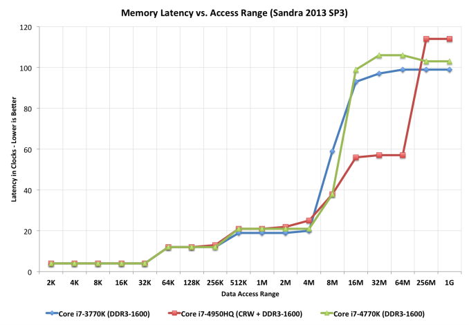
The L3 cache is now back on its own power/frequency plane, although most of the time it seems to run in lockstep with the CPU cores. There appears to be a 2 - 3 cycle access penalty as a result of decoupling the L3 cache.
Power Improvements
Although Haswell’s platform power is expected to drop considerably in mobile, particularly with Haswell U and Y SKUs (Ultrabooks and ultrathins/tablets), there are benefits to desktop Haswell parts as well.
There’s more fine grained power gating, lower chipset power and the CPU cores can transition between power states about 25% quicker than in Ivy Bridge - allowing the power control unit to be more aggressive in selecting lower power modes. We’ve also seen considerable improvements on lowering platform power consumption at the motherboard level as well. Using ASUS’ Z77 Deluxe and Z87 Deluxe motherboards for the Haswell, Ivy and Sandy Bridge CPUs, I measured significant improvements in idle power consumption:
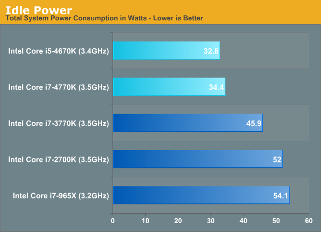
These savings are beyond what I’d expect from Haswell alone. Intel isn’t the only one looking to make things as best as can be in the absence of any low hanging fruit. The motherboard makers are aggressively polishing their designs in order to grow their marketshare in a very difficult environment.
Under load, there’s no escaping the fact that Haswell can burn more power in pursuit of higher performance:
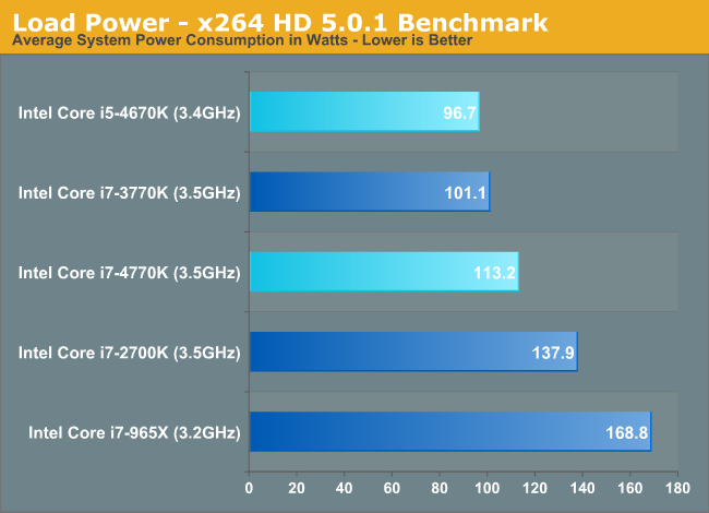
Here I’m showing an 11.8% increase in power consumption, and in this particular test the Core i7-4770K is 13% faster than the i7-3770K. Power consumption goes up, but so does performance per watt.
The other big part of the Haswell power story is what Intel is calling FIVR: Haswell’s Fully Integrated Voltage Regulator. Through a combination of on-die and on-package circuitry (mostly inductors on-package), Haswell assumes responsibility of distributing voltages to individual blocks and controllers (e.g. PCIe controller, memory controller, processor graphics, etc...). With FIVR, it’s easy to implement tons of voltage rails - which is why Intel doubled the number of internal voltage rails. With more independent voltage rails, there’s more fine grained control over the power delivered to various blocks of Haswell.
Thanks to a relatively high input voltage (on the order of 1.8V), it’s possible to generate quite a bit of current on-package and efficiently distribute power to all areas of the chip. Voltage ramps are 5 - 10x quicker with FIVR than with a traditional on-board voltage regulator implementation.
In order to ensure broad compatibility with memory types, there’s a second input voltage for DRAM as well.
FIVR also comes with a reduction in board area and component cost. I don’t suppose this is going to be a huge deal for desktops (admittedly the space and cost savings are basically non-existent), but it’ll mean a lot for mobile.
No S0ix for Desktop
You’ll notice that I didn’t mention any of the aggressive platform power optimizations in my sections on Haswell power management, that’s because they pretty much don’t apply here. The new active idle (S0ix) states are not supported by any of the desktop SKUs. It’s only the forthcoming Y and U series parts that support S0ix.
Memory
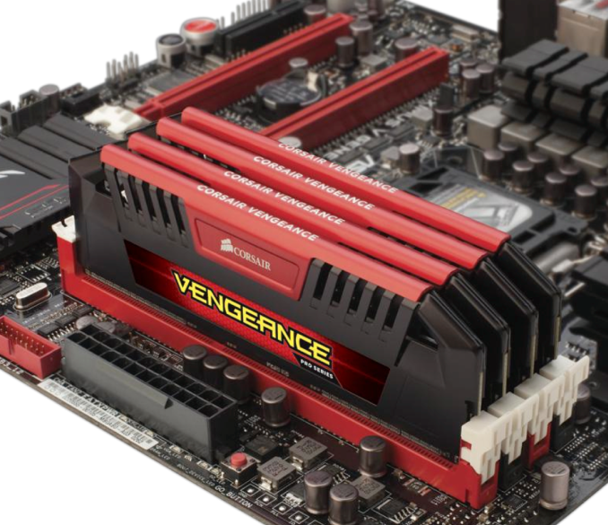
Haswell got an updated memory controller that’s supposed to do a great job of running at very high frequencies. Corsair was kind enough to send over some of its Vengeance Pro memory with factory DDR3-2400 XMP profiles. I have to say, the experience was quite possibly the simplest memory overclocking I’ve ever encountered. Ivy Bridge was pretty decent at higher speeds, but Haswell is a different beast entirely.
Although I used DDR3-2400 for most of my testing, Corsair’s Vengeance Pro line is available in frequencies rated all the way up to 2933MHz.
Platform
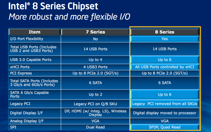
Haswell features a new socket (LGA-1150). Fundamental changes to power delivery made it impossible to maintain backwards compatibility with existing LGA-1155 sockets. Alongside the new socket comes Intel’s new 8-series chipsets.
At a high level the 8-series chipsets bring support for up to six SATA 6Gbps and USB 3.0. It’s taken Intel far too long to move beyond two 6Gbps SATA ports, so this is a welcome change. With 8-series Intel also finally got rid of legacy PCI support.
Overclocking
Despite most of the voltage regulation being moved on-package, motherboards still expose all of the same voltage controls that you’re used to from previous platforms. Haswell’s FIVR does increase the thermal footprint of the chip itself, which is why TDPs went up from 77W to 84W at the high-end for LGA-1150 SKUs. Combine higher temperatures under the heatspreader with a more mobile focused chip design, and overclocking is going to depend on yield and luck of the draw more than it has in the past.
Haswell doesn’t change the overclocking limits put in place with Sandy Bridge. All CPUs are frequency locked, however K-series parts ship fully unlocked. A new addition is the ability to adjust BCLK to one of three pre-defined straps (100/125/167MHz). The BCLK adjustment gives you a little more flexibility when overclocking, but you still need a K-SKU to take advantage of the options.
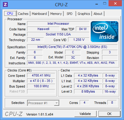

In terms of overclocking success on standard air cooling you should expect anywhere from 4.3GHz - 4.7GHz at somewhere in the 1.2 - 1.35V range. At the higher end of that spectrum you need to be sure to invest in a good cooler as you’re more likely to bump into thermal limits if you’re running on stable settings.
The Launch Lineup: Quad Cores For All
As was the case with the launch of Ivy Bridge last year, Intel is initially launching with their high-end quad core parts, and as the year passes on will progressively rollout dual cores, low voltage parts, and other lower-end parts. That means the bigger notebooks and naturally the performance desktops will arrive first, followed by the ultraportables, Ultrabooks and more affordable desktops. One change however is that Intel will be launching their first BGA (non-socketed) Haswell part right away, the Iris Pro equipped i7-4770R.
| Intel 4th Gen Core i7 Desktop Processors | ||||||
| Model | Core i7-4770K | Core i7-4770 | Core i7-4770S | Core i7-4770T | Core i7-4770R | Core i7-4765T |
| Cores/Threads | 4/8 | 4/8 | 4/8 | 4/8 | 4/8 | 4/8 |
| CPU Base Freq | 3.5 | 3.4 | 3.1 | 2.5 | 3.2 | 2.0 |
| Max Turbo | 3.9 (Unlocked) | 3.9 | 3.9 | 3.7 | 3.9 | 3.0 |
| Test TDP | 84W | 84W | 65W | 45W | 65W | 35W |
| HD Graphics | 4600 | 4600 | 4600 | 4600 | Iris Pro 5200 | 4600 |
| GPU Max Clock | 1250 | 1200 | 1200 | 1200 | 1300 | 1200 |
| L3 Cache | 8MB | 8MB | 8MB | 8MB | 6MB | 8MB |
| DDR3 Support | 1333/1600 | 1333/1600 | 1333/1600 | 1333/1600 | 1333/1600 | 1333/1600 |
| vPro/TXT/VT-d/SIPP | No | Yes | Yes | Yes | No | Yes |
| Package | LGA-1150 | LGA-1150 | LGA-1150 | LGA-1150 | BGA | LGA-1150 |
| Price | $339 | $303 | $303 | $303 | OEM | $303 |
Starting at the top of the product and performance stack, we have the desktop Core i7 parts. All of these CPUs feature Hyper-Threading Technology, so they’re the same quad-core with four virtual cores that we’ve seen since Bloomfield hit the scene. The fastest chip for most purposes remains the K-series 4770K, with its unlocked multiplier and slightly higher base clock speed. Base core clocks as well as maximum Turbo Boost clocks are basically dictated by the TDP, with the 4770S being less likely to maintain maximum turbo most likely, and the 4770T and 4765T giving up quite a bit more in clock speed in order to hit substantially lower power targets.
It’s worth pointing out that the highest “Test TDP” values are up slightly relative to the last generation Ivy Bridge equivalents—84W instead of 77W. Mobile TDPs are a different matter, and as we’ll discuss elsewhere they’re all 2W higher, but that is further offset by the improved idle power consumption Haswell brings.
Nearly all of these are GT2 graphics configurations (20 EUs), so they should be slightly faster than the last generation HD 4000 in graphics workloads. The one exception is the i7-4770R, which is also the only chip that comes in a BGA package. The reasoning here is simple if perhaps flawed: if you want the fastest iGPU configuration (GT3e with 40 EUs and embedded DRAM), you’re probably not going to have a discrete GPU and will most likely be purchasing an OEM desktop. Interestingly, the 4770R also drops the L3 cache down to 6MB, and it’s not clear whether this is due to it having no real benefit (i.e. the eDRAM functions as an even larger L4 cache), or if it’s to reduce power use slightly, or Intel may have a separate die for this particular configuration. Then again, maybe Intel is just busily creating a bit of extra market segmentation.
Not included in the above table are all the common features to the entire Core i7 line: AVX2 instructions, Quick Sync, AES-NI, PCIe 3.0, and Intel Virtualization Technology. As we’ve seen in the past, the K-series parts (and now the R-series as well) omit support for vPro, TXT, VT-d, and SIPP from the list. The 4770K is an enthusiast part with overclocking support, so that makes some sense, but the 4770R doesn’t really have the same qualification. Presumably it’s intended for the consumer market, as businesses are less likely to need the Iris Pro graphics.
| Intel 4th Gen Core i5 Desktop Processors | ||||||
| Model | Core i5-4670K | Core i5-4670 | Core i5-4670S | Core i5-4670T | Core i5-4570 | Core i5-4570S |
| Cores/Threads | 4/4 | 4/4 | 4/4 | 4/4 | 4/4 | 4/4 |
| CPU Base Freq | 3.4 | 3.4 | 3.1 | 2.3 | 3.2 | 2.9 |
| Max Turbo | 3.8 (Unlocked) | 3.8 | 3.8 | 3.3 | 3.6 | 3.6 |
| Test TDP | 84W | 84W | 65W | 45W | 84W | 65W |
| HD Graphics | 4600 | 4600 | 4600 | 4600 | 4600 | 4600 |
| GPU Max Clock | 1200 | 1200 | 1200 | 1200 | 1150 | 1150 |
| L3 Cache | 6MB | 6MB | 6MB | 6MB | 6MB | 6MB |
| DDR3 Support | 1333/1600 | 1333/1600 | 1333/1600 | 1333/1600 | 1333/1600 | 1333/1600 |
| vPro/TXT/VT-d/SIPP | No | Yes | Yes | Yes | Yes | Yes |
| Package | LGA-1150 | LGA-1150 | LGA-1150 | LGA-1150 | LGA-1150 | LGA-1150 |
| Price | $242 | $213 | $213 | $213 | $192 | $192 |
The Core i5 lineup basically rehashes the above story, only now without Hyper-Threading. For many users, Core i5 is the sweet spot of price and performance, delivering nearly all the performance of the i7 models at 2/3 the price. There aren’t any Iris or Iris Pro Core i5 desktop parts, at least not yet, and all of the above CPUs are using the GT2 graphics configuration. As above, the K-series part also lacks vPro/TXT/VT-d support but comes with an unlocked multiplier.
Obviously we’re still missing all of the Core i3 parts, which are likely to be dual-core once more, along with some dual-core i5 parts as well. These are probably going to come in another quarter, or at least a month or two out, as there’s no real need for Intel to launch their lower cost parts right now. Similarly, we don’t have any Celeron or Pentium Haswell derivatives launching yet, and judging by the Ivy Bridge rollout I suspect it may be a couple quarters before Intel pushes out ultra-budget Haswell chips. For now, the Ivy Bridge Celeron/Pentium parts are likely as low as Intel wants to go down the food chain for their “big core” architectures.
For those interested in the mobile side of things, we’ve broken out those parts into a separate Pipeline article.
Die Size and Transistor Count
Moving on to die sizes and transistor counts, this year Intel is striving to be more straightforward and accurate than was the case with Sandy Bridge and Ivy Bridge. With the Bridge generation we didn’t initially get comparable numbers, only for the correction to throw in additional confusion. For Haswell Intel is laying things out from the start, listing both possible numbers so that either can be compared.
| CPU Specification Comparison | |||||||||
| CPU | Manufacturing Process | Cores | GPU | Transistor Count (Schematic) | Die Size | ||||
| Haswell GT3 4C | 22nm | 4 | GT3 | ? | 264mm2 (est) | ||||
| Haswell GT2 4C | 22nm | 4 | GT2 | 1.4B | 177mm2 | ||||
| Haswell ULT GT3 2C | 22nm | 2 | GT3 | 1.3B | 181mm2 | ||||
| Intel Ivy Bridge 4C | 22nm | 4 | GT2 | 1.2B | 160mm2 | ||||
| Intel Sandy Bridge E 6C | 32nm | 6 | N/A | 2.27B | 435mm2 | ||||
| Intel Sandy Bridge 4C | 32nm | 4 | GT2 | 995M | 216mm2 | ||||
| Intel Lynnfield 4C | 45nm | 4 | N/A | 774M | 296mm2 | ||||
| AMD Trinity 4C | 32nm | 4 | 7660D | 1.303B | 246mm2 | ||||
| AMD Vishera 8C | 32nm | 8 | N/A | 1.2B | 315mm2 | ||||
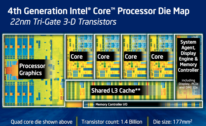
The two numbers for the most common Haswell configuration, Haswell GT2 4C, are 1.4 billion schematic transistors and 1.6 billion layout transistors. Why and what is the difference? The former count is the number of transistors in the schematic (hence the name), and is generally the number we go by when quoting transistor counts. Meanwhile the second number, the layout number, is the number of transistors used in the fabrication process itself. The difference comes from the fact that while the schematic will use one large transistor – being a logical diagram – production will actually use multiple transistors laid out in parallel for layout and process reasons. So how many transistors does Haswell have? It has both 1.4B and 1.6B, depending on which number we’re after, with 1.4B being the number Intel is passing around.
In any case, even among quad cores Haswell is going to come in a couple of different sizes. Along with the 1.4B transistor, 177mm2 4C/GT2 version of Haswell, there is the 4C/GT3 version of Haswell, which Intel doesn’t list the die size or transistor count for. Based on our rough measurements of the physical die we’re at 264mm2, which including the epoxy covering the die will run a bit large.
Breaking things down to the GPU portion of Haswell, based in turn on these measurements I came up with an 87mm^2 adder for the extra hardware in Haswell GT3 vs. GT2. Doubling that 87mm^2 we get a rough idea of how big the full 40 EU Haswell GPU might be: 174mm^2. If my math is right, this means that in a quad-core Haswell GT3 die, around 65% of the die area is GPU. This is contrary to the ~33% in a quad-core Haswell GT2. I suspect a dual-core + GT3 design is at least half GPU. Meanwhile Crystalwell, the 128MB eDRAM, adds another 84mm2 die (by our measurements) to the entire package.
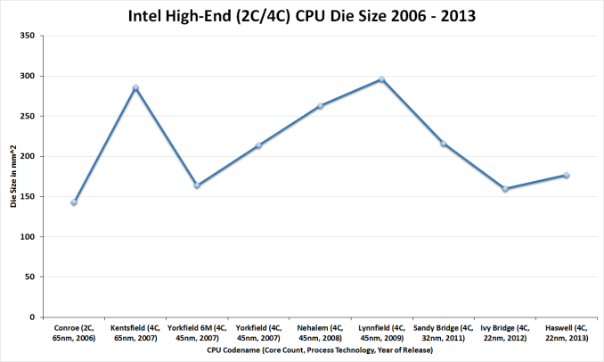
On a comparative basis, the 4C/GT2 version of Haswell is roughly 200M transistors and 17mm2 bigger than the comparable 4C/GT2 version of Ivy Bridge. The transistor count increase is roughly what we’d expect, with most of those transistors going to Haswell itself while the GPU remains relatively unchanged. Though it’s interesting to note that while this marks a 17% increase in transistors, it’s only an 11% increase in die size. Ivy Bridge was a small die for an Intel, and while Haswell grows larger in exchange for the additional functionality the new architecture provides, it’s still a fairly small GPU and reaches a density greater than Ivy Bridge itself. Or to put this another way, Intel’s last tock CPU, Sandy Bridge, was larger still by almost 40mm2. It’s only once we start adding the relatively big GT3 GPU, and not the CPU, that we see Intel go well above 200mm2.
CPU Performance: Five Generations of Intel CPUs Compared
For the purposes of our look at Haswell, we will be breaking up our review coverage into two parts. The rest of this article will focus on the CPU side of Haswell, while coverage of the GPU - including Iris Pro and Crystalwell - has been spun off into another artice: Intel Iris Pro 5200 Graphics Review: Core i7-4950HQ Tested.
The majority of the market doesn’t upgrade annually, so I went back a total of five generations to characterize Haswell’s CPU performance. Everything from a 2.53GHz Core 2 Duo through Nehalem, Sandy Bridge, Ivy Bridge and Haswell are represented here. With the exception of the Core 2 platform, everything else is running at or near the peak launch frequency for the chip.
In general, I saw performance gains over Ivy Bridge of 1 - 19%, with an average improvement of 8.3%. Some of the performance gains were actually quite impressive. The 7.8% increase in Kraken shows there’s still room for improvement in lightly threaded performance, while the double digit FP performance gains in POV-Ray and x264 HD really play to Haswell’s strengths.
Compared to Sandy Bridge, Haswell looks even more impressive. The Core i7-4770K outperforms the i7-2700K by 7 - 26%, with an average performance advantage of 17%. The gains over Sandy Bridge aren’t large enough to make upgrading from a Sandy Bridge i7 to a Haswell i5 worthwhile though, as you still give up a lot if you go from 8 to 4 threads on a quad-core part running heavily threaded workloads.
Compared to Nehalem the gains average almost 44%.
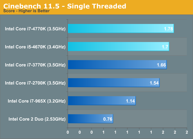
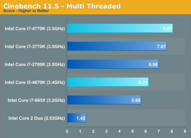
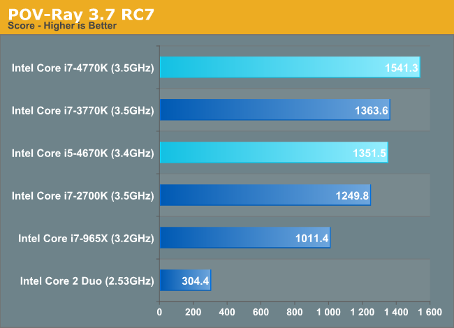
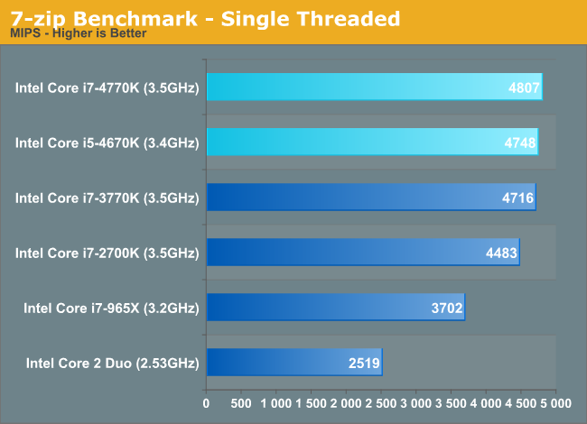
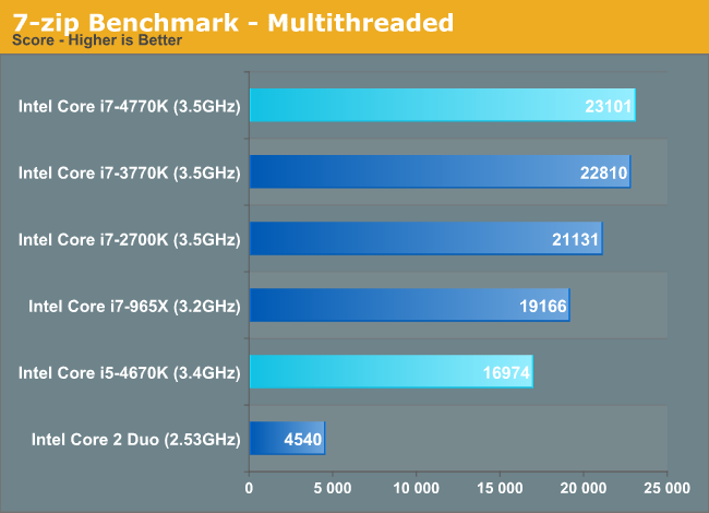
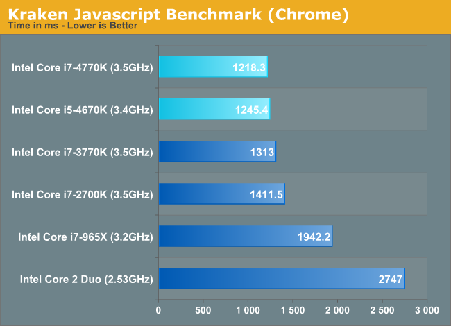
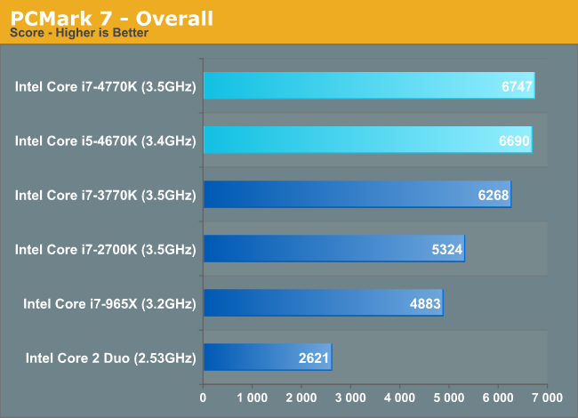
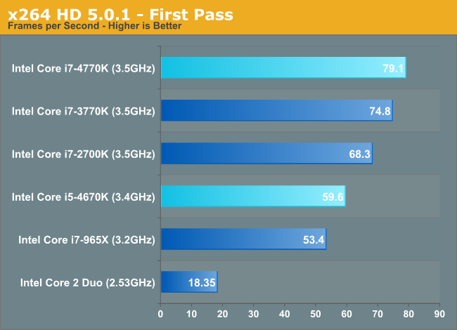
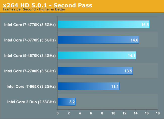
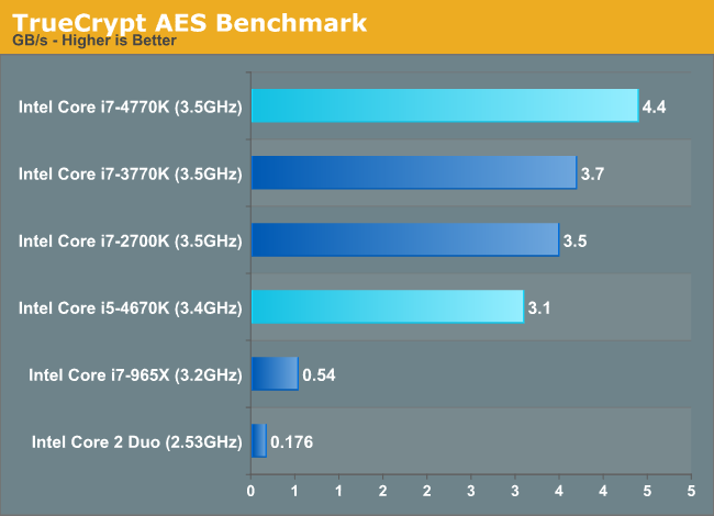
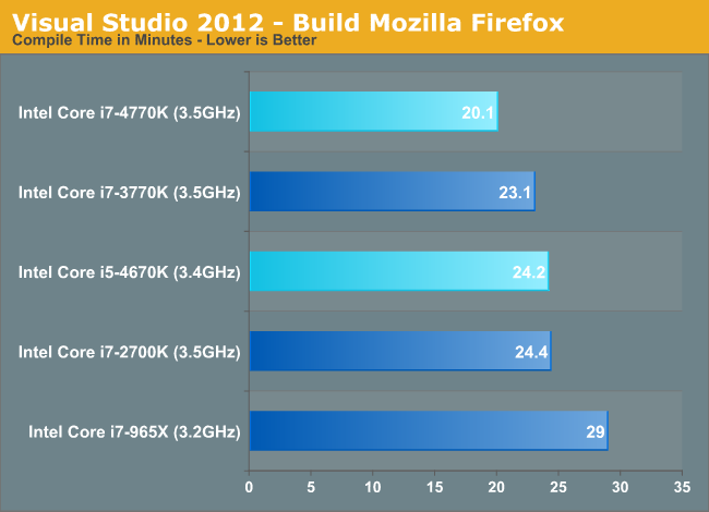
Quite possibly the most surprising was just how consistent (and large) the performance improvements were in our Visual Studio 2012 compile test. With a 15% increase in performance vs. Ivy Bridge at the same frequencies, what we’re looking at here is the perfect example of Haswell’s IPC increases manifesting in a real-world benchmark.
Gaming Performance
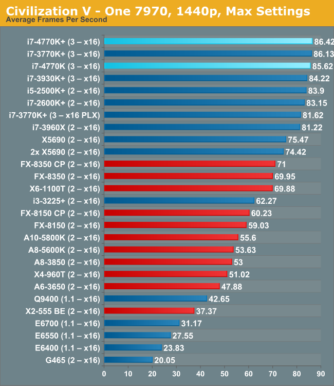
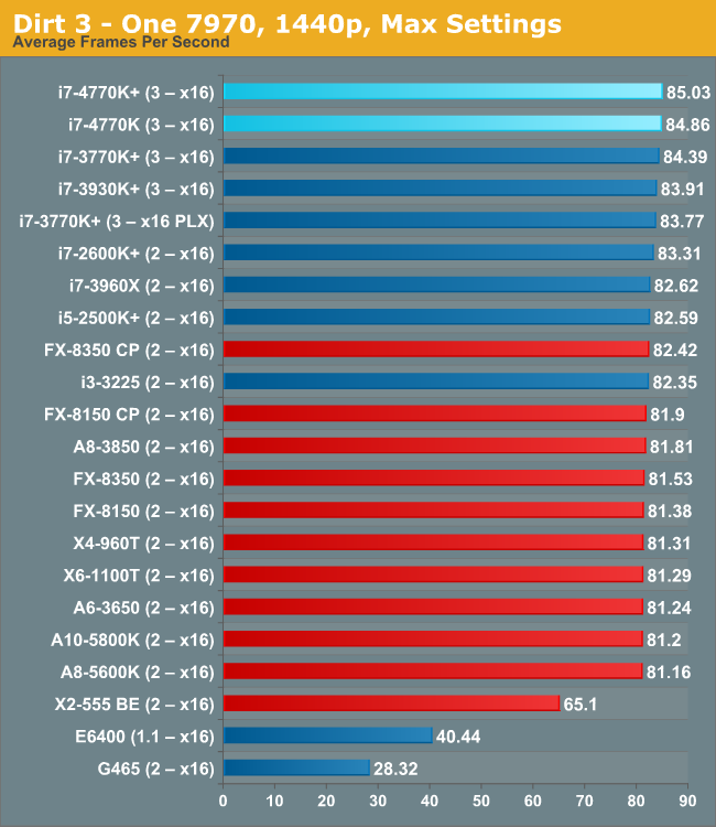
After spending far too much time on the Iris Pro test system, I didn’t have a ton of time left over to do a lot of gaming performance testing with Haswell. Luckily Ian had his gaming performance test data already in the engine, so I borrowed a couple of graphs.
As expected, Haswell is incrementally quicker in GPU bound gaming scenarios compared to Ivy Bridge - and most definitely at the top of the charts.
CPU Performance: Going Even Further Back
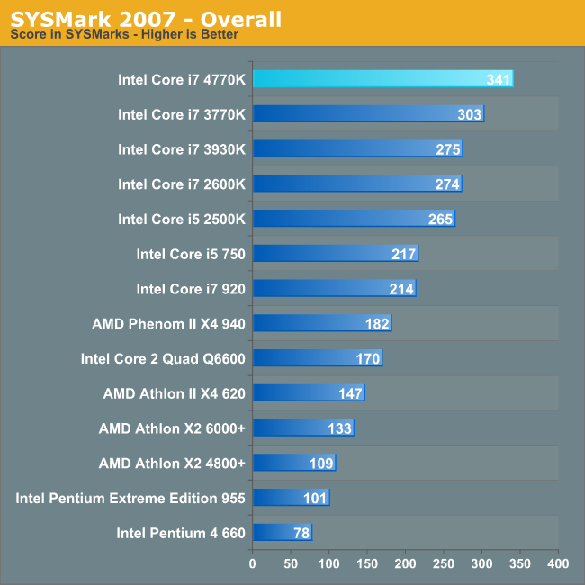
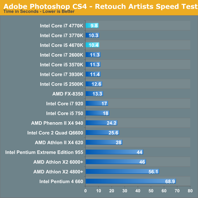
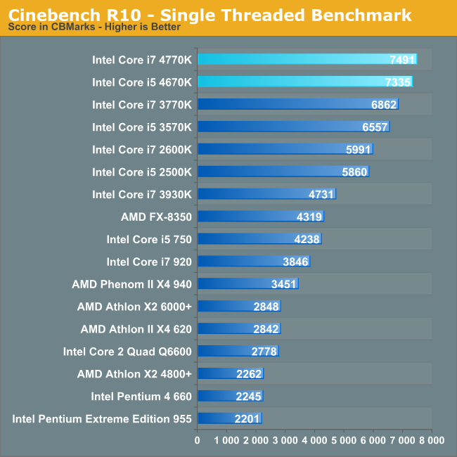
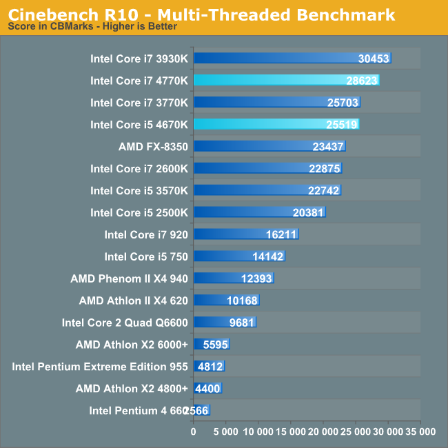
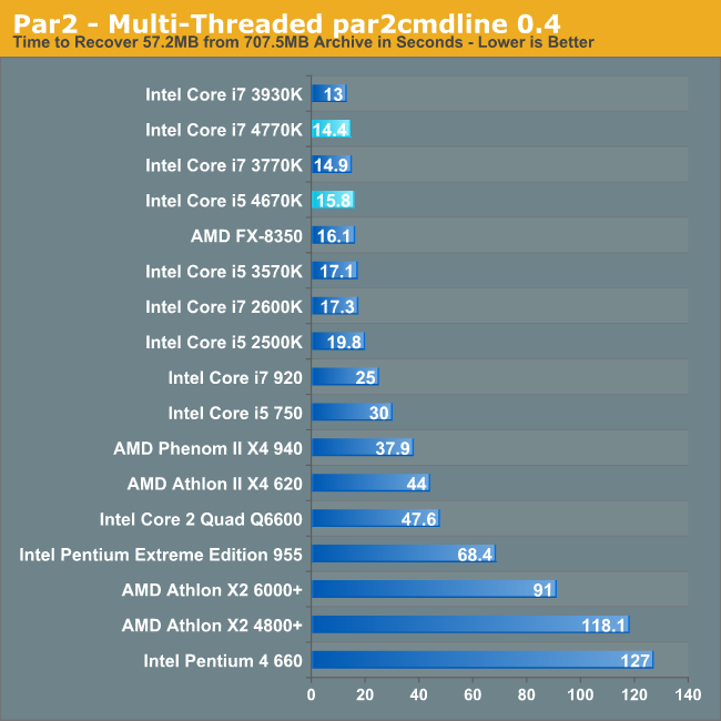
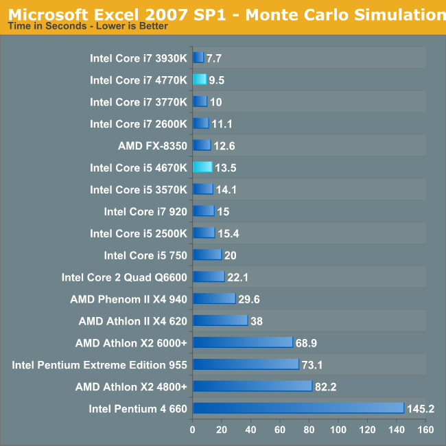
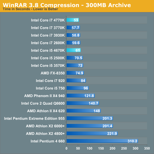
If you want specific comparisons to other CPUs, all of the Haswell data is in Bench. I took the liberty of putting together a few charts comparing the 4770K to some key older parts to put its performance in perspective.
Quick Sync Performance
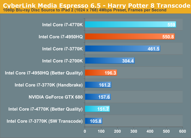
With more graphics EUs under the hood of all desktop Haswells (at least those launching today), Quick Sync performance improves a bit over Ivy Bridge. Intel claims to have focused heavily on improving the quality of Quick Sync transcodes however in my testing I saw a slight regression in quality. I didn’t have a ton of time to dig further to find out what’s going on but I plan on doing so post-Computex. Update: It looks like I wasn't alone in seeing an image quality regression. Haswell QSV image quality is worse than on IVB as Ganesh found.
The other big news is Handbrake now officially supports Quick Sync, something Ganesh will be testing with his HTPC look at Haswell.
Needless to say, Quick Sync performance is better on Haswell than on Ivy Bridge. And it’s even better if you happen to have a Haswell with a 128MB L4 cache.
Final Words
I’m a fan of Haswell, even on the desktop. The performance gains over Ivy Bridge depend on workload, but in general you’re looking at low single digits to just under 20%. We saw great behavior in many of our FP heavy benchmarks as well as our Visual Studio compile test. If you’re upgrading from Sandy Bridge you can expect to see an average improvement just under 20%, while coming from an even older platform like Nehalem will yield closer to a 40% increase in performance at the same clocks. As always, annual upgrades are tough to justify although Haswell may be able to accomplish that in mobile.
Even on the desktop, idle power reductions are apparent both at the CPU level and at the platform level. Intel focused on reducing CPU power, and it seems like Intel's motherboard partners did the same as well. Under load Haswell can draw more power than Ivy Bridge but it typically makes up for it with better performance.
Overclockers may be disappointed at the fact that Haswell is really no more of an overclocker (on air) compared to Ivy Bridge. Given the more mobile focused nature of design, and an increased focus on eliminating wasted power, I don’t know that we’ll ever see a return to the heyday of overclocking.
If the fact that you can’t easily get tons of additional frequency headroom at marginal increase to CPU voltage is the only real downside to the platform, then I’d consider Haswell a success on the desktop. You get more performance and a better platform at roughly the same prices as Ivy Bridge a year ago. It’s not enough to convince folks who just bought a PC over the past year or two to upgrade again, but if you are upgrading from even a 3 year old machine the performance gains will be significant.

